What Is a PCB?
We’re doing a hack day for Friday the 13th / Halloween, and a colleague asked: What is a PCB? What are they used for? Why do we need them?
What
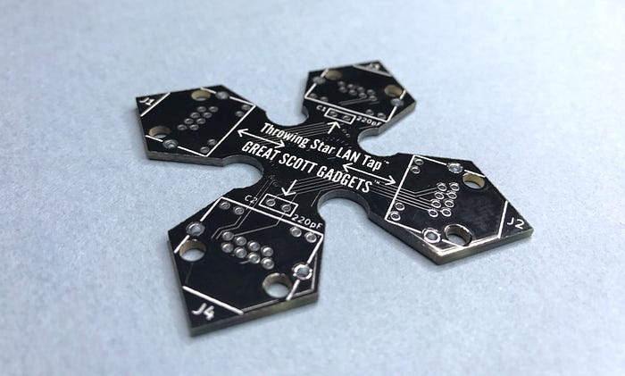
PCB stands for printed circuit board. It’s the next step beyond a breadboard: like a template with all the wires already laid out, just waiting for you to solder on the components. A proto-board is also a PCB, usually laid out like a breadboard, and you apply solder instead of plugging wires in.
Pretty much any electronic circuit you’ll use is mounted on a PCB. It’s the physical foundation of the circuit, the core of the Arduino. All the electrical components of the circuit are wired together via copper traces (which can also be made out of gold or other conductive materials).

Anatomy
Core: The base of the PCB is usually a sheet of fiberglass saturated with resin. It’s usually beige, and is the majority of the thickness of the board. You might hear this called prepreg: this means “pre-impregnated”, fiberglass that was filled with resin before it was heated and hardened. Fun fact: some types of prepreg fluoresce blue or green in UV light! There are also flexible PCBs, which can be made with kapton tape or other materials.
Copper: A layer of conductive metal, usually copper or gold. You’ll mostly find pours, big flat areas of copper (usually connecting things to ground), and traces, thinner “wires” connecting components. Occasionally, you will also find vias — small holes through the PCB itself, connecting pours on different layers.
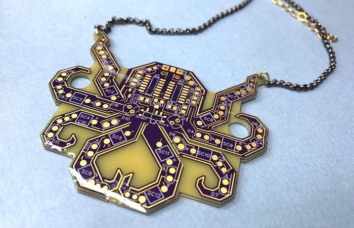
Solder mask: Before, this was pretty much always green. You’ll also find some really old circuit boards without any solder mask at all. Now, solder mask comes in all kinds of colors — including transparent. OSH Park uses a signature shade of purple.
Silk screening: Usually white, this is ink screenprinted on top of the solder mask for labels and branding. Yes, like how T-shirts are made.
Some PCBs have more than one layer. A single-layer PCB has a single copper pour on one side. A double-layer one (like most Arduinos) has copper and components on both sides. But you can also add more layers: a 3-layer board has another layer of fiberglass and another of copper, like a double-decker sandwich. I’ve heard of ones that go all the way up to 16!
You’ll also see varying thicknesses: regular and half-height are the most common. (SparkFun’s LilyPad series are all half-height PCBs.)

Through-Hole vs. Surface-Mount
Does your PCB have biggish holes through it, exposed flat copper pads, or both?
Through-hole soldering is typically used for big components, ones that need structural stability, or kits. It’s often easier for beginners, and requires less precision than surface-mount.
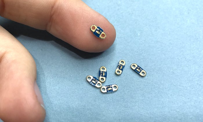
Surface-mount soldering is used for small components, so you’ll see it on most commercial boards. There are no holes going through the board; the component sits on top of the surface. SMT = surface-mount technology, and SMD = surface-mount device. Most sewable LEDs consist of surface-mount LEDs and resistors attached to a PCB, with exposed pads on each end with big holes through them.

Chips are a special case. You might hear of BGA technology: this stands for Ball-Grid Array, a system of surface-mount pads on the PCB that correspond to metal beads on the bottom of a chip, which means the chip can have more connections and a smaller footprint. If you’re doing through-hole soldering, you’ll usually solder a socket onto the board and then place the chip in it later, so that you don’t cause heat damage.
There’s all kinds of tutorials on how to solder through-hole and surface-mount circuits. Here’s a quick video on each:
Through-hole
Surface-mount
Making Your Own
Routing: Perhaps the simplest to understand is routing. It starts with a copper clad board: fiberglass with copper on one or both sides. You use a router—basically a computer-controlled, movable drill—to cut channels in the copper, to create big areas or smaller traces, connecting and separating parts of the board. (You might hear “CNC”, referring to Computer Numerical Control. This covers any tool that is controlled by a ‘puter, such as a router, mill, lathe, laser cutter, or 3D printer.)
Etching: This is similar to routing, except you use a chemical etchant to eat away the copper. You use a mask to block off areas where the copper should remain; a couple of methods include Sharpie and toner transfer (which simply requires an office printer and an iron).
With routing or etching, you can buy liquid solder mask to apply over the copper. It usually requires UV light to cure.
CAD software: CAD stands for Computer Aided Design, and is a genre of software used to create files for PCBs, 3D printing, laser cutting, etc… In this case, you have a few great options. Autodesk Eagle is a solid standard. KiCAD is free and open-source, so very popular with the DIY hardware crowd, plus it holds its own against Eagle. Altium owns CircuitMaker — a lighter option available for Windows — and Upverter, a browser-based suite geared toward collaboration. There’s also one created especially for art, called PCBmodE. Most of these have excellent tutorials available; we recommend Sparkfun’s Eagle tutorial and Chris Gammell’s Getting to Blinky for KiCAD.
Once you’ve created your PCB, you can send it off to a shop like OSH Park to get it made. Depending on the service you use, you may be able to pay extra to have to board populated with parts, so it arrives already assembled. (But that takes out some of the fun, right?) From there, you could go on to sell your PCB as a kit on CrowdSupply, Tindie, or GroupGets… even Kickstarter!
Have fun, and solder on! 😃

